 HC PHOTONICS CORP社
PPLN Chips/Custom PPLN
PPLN (ridge) waveguide
HC Photonics Corp. is specialized at poling technique on a ferro-electric material. Not only the conventional quasi-phase matching (QPM) devices which often are periodically poled structures, non-periodic pattern or custom pattern are also available with our state-of-art poling technique.
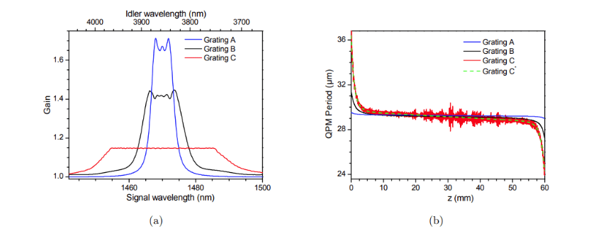
A typical aperiodic pattern is the period chirped grating, in which the period is increase or decrease along the length of chip linearly or non-linearly. By sweeping the period range, one can determine the spectral components to be phase-matched and resulting in a wide phase matching bandwidth.
Fig. 1 Theoretical single-pass, small-signal parametric gain spectra (a) and corresponding QPM domain widths (half periods) (b) for gratings A, B and C, respectively in grey, black and red. Grating C domain widths are calculated using Lai et al. algorithm to improve the flatness of the gain spectrum. (figure ref. from [1])
[1]. Quantum Sensing and Nano Electronics and Photonics XIV 10111, 101112X
In fact, the phase-matching (PM) response can be tailored by properly engineering the domain orientation of a QPM superlattice. For example, simultaneously phase-matching for multi-wavelengths second harmonic generation (SHG) with desired wavelength and weighting in an aperiodically poled grating are demonstrated by Lai et al . Not only fabricate the PPLN device, HCP also provide the service for aperiodically poled grating design for desired phase-matching response such as multi-wavelength SHG, broadband phase-matching…etc.
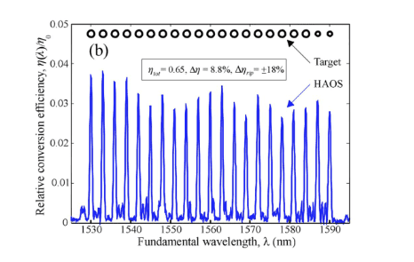
Fig. 2 Experimentally measured PM tuning curves designed for target spectra of 21 peaks SHG (open circles).
OPTICS LETTERS 37, 1184-1187 (2012).
Additional to the 1-D grating for tailored-made spectral PM response, spatial distribution such as beam shaping is feasible by a 2-D poled PPLN. By introducing the concept of holography into nonlinear frequency mixing, one can design the spatial shape of the frequency converted waves such as Top-Hat beam.
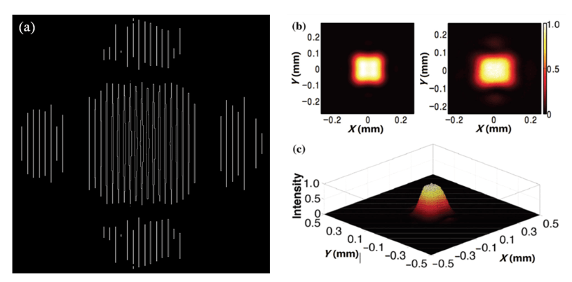
Fig 3(a). The designed mask pattern for Top-Hat beam shaping. (b). A comparison between simulated (left) and measured (right) SH Top-Hat beams, figure ref. from [3].
Shapira, A., Naor, L. & Arie, A. Sci. Bull. (2015) 60: 1403.
We understand that a conventional PPLN might not satisfy some advance applications, so we quite welcome the custom design pattern and would like to spend the effort to push the limitation of domain engineering and poling technique.